What is strained layer epitaxy?
What is strained layer epitaxy?
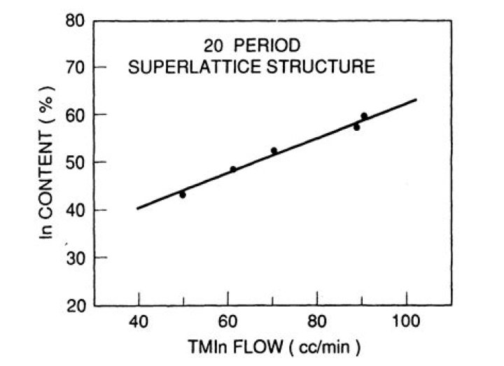
Strained layer epitaxy is a process for the formation of new materials with a strain and composition modulation in the one to one hundred monolayer range.
What is strained layer?
In strained-layer epitaxy, the strain energy (resulting from lattice mismatch, f) between the substrate and the epitaxially grown overlayer, or epi-layer, controls growth. Typically, the epi-layer is biaxially strained in the plane of the substrate and uniaxially strained in the perpendicular direction.
What is channel strain engineering?
Strain engineering refers to a general strategy employed in semiconductor manufacturing to enhance device performance. Performance benefits are achieved by modulating strain in the transistor channel, which enhances electron mobility (or hole mobility) and thereby conductivity through the channel.
What is epitaxy and its types?
Epitaxy refers to a type of crystal growth or material deposition in which new crystalline layers are formed with one or more well-defined orientations with respect to the crystalline seed layer. The term epitaxy comes from the Greek roots epi (ἐπί), meaning “above”, and taxis (τάξις), meaning “an ordered manner”.
What is Strained silicon technology?
Strained silicon is a layer of silicon in which the silicon atoms are stretched beyond their normal interatomic distance. This can be accomplished by putting the layer of silicon over a substrate of silicon germanium (SiGe). These electrons can move 70% faster allowing strained silicon transistors to switch 35% faster.
What is the purpose of strained silicon?
A primary purpose for applying tensile strain in Si is to improve its electronic properties; the strain reduces carrier scattering and the effective transport mass of electrons.
What is strain in mechanical engineering?
Strain is the deformation of a material from stress. It is simply a ratio of the change in length to the original length. Deformations that are applied perpendicular to the cross section are normal strains, while deformations applied parallel to the cross section are shear strains.
What is strain definition in engineering?
strain, in physical sciences and engineering, number that describes relative deformation or change in shape and size of elastic, plastic, and fluid materials under applied forces. In the case of elongation, or lengthwise compression, the normal strain is equal to the change in length divided by the original length.
Why epitaxy is required?
The commercial importance of epitaxy comes mostly from its use in the growth of semiconductor materials for forming layers and quantum wells in electronic and photonic devices—for example, in computer, video display, and telecommunications applications.
Why epitaxy is done?
Silicon epitaxy is done to improve the performance of bipolar devices. By growing a lightly doped epi layer over a heavily-doped silicon substrate, a higher breakdown voltage across the collector-substrate junction is achieved while maintaining low collector resistance.
What is strained silicon semiconductor?
Strained silicon is a layer of silicon in which the silicon atoms are stretched beyond their normal interatomic distance. More recent methods of inducing strain include doping the source and drain with lattice mismatched atoms such as germanium and carbon.