Where does Fermi level lies in p-type semiconductor?
valence band
Fermi level in n-type semiconductor lies near the conduction band or in p-type semiconductor lies near in the valence band.
Where does the Fermi level lies in an extrinsic semiconductor?
Fermi level in extrinsic semiconductor. In extrinsic semiconductor, the number of electrons in the conduction band and the number of holes in the valence band are not equal. Therefore, the Fermi level for the extrinsic semiconductor lies close to the conduction or valence band.
Where will be the Fermi energy for intrinsic and extrinsic semiconductors in terms of energy gap?
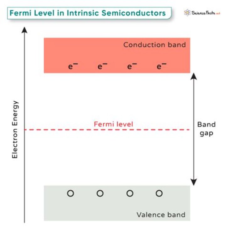
For an intrinsic semiconductor, the electron-carrier concentration is equal to the hole-carrier concentration. Therefore, the Fermi level in an intrinsic semiconductor lies in the middle of the forbidden gap.
What is Fermi energy level in physics?
What is Fermi Level? The highest energy level that an electron can occupy at the absolute zero temperature is known as the Fermi Level. The Fermi level lies between the valence band and conduction band because at absolute zero temperature the electrons are all in the lowest energy state.
Where will the Fermi level be located for a P-type doped semiconductor at a very high temperature in the intrinsic regime )?
Equation 1 can be modified for an intrinsic semiconductor, where the Fermi level is close to center of the band gap (EFi). For a p-type semiconductor with Na donors which are fully ionized, p = Na when Na ≫ ni, so that the Fermi level is shifted below the center of the band gap, closer to the valence band.
What is Fermi energy level in p-type and n-type semiconductor?
Fermi level – the highest energy level that an electron can occupy at absolute 0 temperature. From the energy level diagram of the n-type semiconductor, it’s clear that the Fermi level is present near the conduction band and far away from the valence band.
What do you mean by Fermi level in semiconductor show that Fermi level lies in midway of forbidden energy gap in intrinsic semiconductor?
In intrinsic semiconductor, the number of holes in valence band is equal to the number of electrons in the conduction band. Hence, the probability of occupation of energy levels in conduction band and valence band are equal. Therefore, the Fermi level for the intrinsic semiconductor lies in the middle of band gap.
How is Fermi energy level calculated?
Fermi energy: Ef = ħ² * kf² / (2 * m) Fermi velocity: vf = ħ * kf / m. Fermi temperature: Tf = Ef / k….
- n is the number density,
- m is the electron mass m = 9.10938356 * 10^(-31) kg ,
- k is the Boltzmann constant k = 1.38064852 * 10^(-23) m² * kg / (s² * K) .
What do you mean by Fermi level in semiconductor?
The Fermi Level is the energy level which is occupied by the electron orbital at temperature equals 0 K. The level of occupancy determines the conductivity of different materials. These orbitals, combined with the energy level, determine whether the material is an insulator, semi-conductor, or conductor.
What is meant by Fermi level in semiconductor Where does Fermi level lies in intrinsic semiconductor?
What is Fermi energy level in intrinsic semiconductor?
Concept: Fermi Level: The Fermi-level in an intrinsic semiconductor is nearly midway between the conductive and valence band. Fermi level is the highest energy state occupied by electrons in a material at absolute zero temperature.
Where the Fermi energy level does lies in n-type semiconductor How does it varies with respect to temperature?
IN n-TYPE SEMICONDUCTOR. At 0K the fermi level E_{Fn} lies between the conduction band and the donor level. As temperature increases more and more electrons shift to the conduction band leaving behind equal number of holes in the valence band.
