What is depletion region in P-N junction diode?
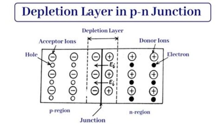
Depletion region or depletion layer is a region in a P-N junction diode where no mobile charge carriers are present. Depletion layer acts like a barrier that opposes the flow of electrons from n-side and holes from p-side.
Where is the depletion region of a P-N junction?
This space-charge region on either side of the junction together is known as the depletion region as the electrons and holes taking part in the initial movement across the junction depleted the region of its free charges.
What is the purpose of depletion region?
The word depletion in English refers to the decrease in the quantity of something. Similarly, in semiconductors, the depletion region is the layer where the flow of charges decreases. This region acts as the barrier that opposes the flow of electrons from the n-side to the p-side of the semiconductor diode.
How does the depletion region of a P-N junction diode get affected?
Essentially, majority carriers are pushed away from the junction, leaving behind more charged ions. Thus the depletion region is widened and its field becomes stronger, which increases the drift component of current (through the junction interface) and decreases the diffusion component.
What is depletion region in a PN junction which process causes depletion region in a PN junction?
The depletion layer in the p-n junction region is caused by diffusion of charge carriers.
What depletion region contains?
Note: The depletion layer consists of both electrons and protons but they are immobile in nature therefore the correct answer would be immobile ions. The donor and acceptor atom get a positive and negative charge due to which the PN junction forms.
What is depletion region in pn junction Class 12?
The region of positive charge and negative charge on either side of the junction is termed as the depletion region.
Which process causes depletion layer in pn junction?
diffusion of charge carriers
The depletion layer in the p-n junction region is caused by diffusion of charge carriers.
What is barrier potential in P-N junction diode?
The potential difference required to move the electrons through the electric field is called the barrier potential. Barrier potential of a P-N junction depends on the type of semiconductor material, amount of doping and temperature. This is approximately 0.7V for silicon and 0.3 V for germanium.
How does the depletion region of pn junction diode gets affected under reverse bias?
When p-n junction is reversed biased, the positive terminal of the external battery is connected to n-side of p-n junction and its negative terminal to p-side of p-n junction. Due to it, the majority charge carriers move away from the junction. This increases the width of the depletion layer.
What is the cause and effect of depletion layer in pn junction?
Due to the larger concentration of electrons in N-side and holes in P-side, they diffuses from their own side to other side. Hence depletion region produces.
What type of particles are available in the depletion region of a pn junction diode?
Depletion layer contains only fixed positive and negative ions, positive ions on n-side and negative ions on p-side.
