How do you calculate current carrying capacity of PCB traces?
Max Current You can calculate maximum current by using the formula A = (T x W x 1.378 [mils/oz/ft2]). The values in this formula correspond with the following parameters: A: Cross-section area.
How much current can a PCB trace handle?
Relationship between Copper Weight, Trace Width and Current Carrying Capacity
| Temp rise | 10°C | 30°C |
|---|---|---|
| Trace width (inch) | Max. current amps | |
| 0.01 | 0.5 | 0.7 |
| 0.015 | 0.7 | 1.0 |
| 0.02 | 0.7 | 1.2 |
How much current can a 10 mil trace carry?
How much current can a 10 mil trace carry? Under the same temperature rise that is 10°C, a 10mil-trace with 1oz copper weight is capable of withstanding current of 1amp at most and we rest assured that a 50mil-trace is capable of withstanding current larger than 1amp.
How wide should PCB traces be?
A standard trace width for an ordinary signal (no special requirements) may be in the 7-12 mil range and be as long as a few inches, but there are many things that should be considered when defining the width and length of a trace.
How much current can a Via carry?
Vias have very low resistance and even a 0.35 mm drill via can safely carry 2 amps of current. Furthermore, their resistance can be reduced by filling them with solder.
What is the standard thickness of a PCB?
What is Standard PCB Thickness? Many contract manufacturers may say that the standard PCB thickness is 1.57 mm, or approximately 0.062 in.
What is trace spacing?
What is the minimum PCB line/trace spacing? The minimum line spacing between PCB components and other traces is the distance required to withstand a given voltage. It is defined in terms of creepage and clearance distances.
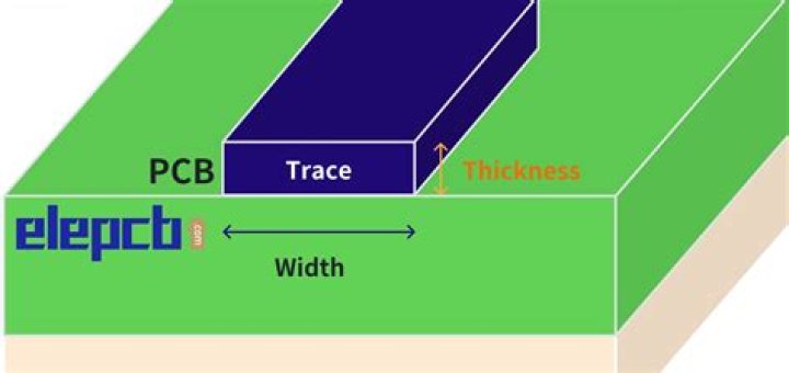
What is PCB trace?
A PCB trace or PCB track is a copper conductor on the PCB that conducts signals on the surface of the PCB. It is the flat, narrow portion of the copper foil that is left behind after etching. The electricity that flows through the copper traces generates a significant amount of heat.
